|
|
Ever since I read K. Eric Drexler's Engines of Creation
I'd been interested in nanotechnology and followed the relevant literature while trying to figure out, as is my wont, how to make a buck out of it. As one of the designers of Xanadu and an ardent supporter of the project, Eric became acquainted with Autodesk when we invested in Xanadu in 1988. When Eric saw a demo of HyperChem at a conference, he immediately realised that the fit between Autodesk and Hypercube, Inc., developers of HyperChem, was potentially very good. When Eric and Chris Peterson spoke to me about this opportunity, I finally saw not only an opportunity for Autodesk to establish itself in the scientific modeling market, but also a way to position ourselves to benefit from the advent of nanotechnology, if and when it emerged, for surely one could not design atomically-precise structures without a molecular CAD system, which is precisely what a molecular modeling package is.
In early 1989, I prepared this talk about the consequences of nanotechnology to help tilt the balance in favour of the HyperChem deal. The talk was delivered at the Autodesk technology forum on May 10, 1990, before an audience which included Eric Drexler, Chris Peterson, and Neil Ostlund, founder and president of HyperCube, the designer of HyperChem.
This talk has been reprinted by the Foresight Institute,
in Micro-Times,
and Mondo 2000.
![[Footnote]](i/footnote.png)
Autodesk Technology Forum Presentation
by John Walker
May 10th, 1990
These are indeed extraordinary times we're living through.
Few people are lucky enough to live at a time when their chosen field of interest becomes the center of a technological revolution that changes the face of the world.
We've all shared that good fortune; the success of Autodesk in so short a time is evidence of of how rapidly and how completely the evolution of computers has changed the way design and engineering are done and has reshaped the very terrain on which businesses compete.
Yet all of these remarkable events were predictable, at least in general outline, more than 25 years ago. I remember, like yesterday, the afternoon in the spring of 1968 when, after I first learned about the technologies used in the crude integrated circuits of the time, it hit me. There was no fundamental physical reason you couldn't put a whole computer on a single chip. It was just a matter of engineering, money, and time.
Now I certainly didn't know when it would happen, and I doubt anybody anticipated price and performance reaching their current levels, but the direction and the goal was clear. It made engineering and economic sense; there was no reason it wouldn't work; and each intermediate step along the way would clearly pay for itself in commercially successful products. That pretty much made it inevitable.
This is the kind of reasoning I'm going to be using in this presentation—projecting readily predictable trends forward and asking the question “How far can we go, and what happens when we get there?”
Some of the conclusions that seem almost inevitable have profound consequences that are not just interesting, but important for companies like Autodesk who wish to grow and prosper in the coming years.
Let's start by looking at the key trend that's driven the entire silicon revolution. It's really very simple: making things smaller, or in engineer-speak, device scaling.
In the early days of transistors, it was observed that when you made a device smaller, you got the best of everything. It ran faster, it used less power and ran cooler, and since you could pack a lot more of them on a single wafer and the cost of processing a wafer was the same regardless of what was on it, the price per device went down.
After the first primitive integrated circuits were made in the late 1950s, the incentive to miniaturise became even more compelling. By reducing the size of devices further, more complex circuitry could be packed onto each chip. And remember, all chips cost roughly the same to make, regardless of what they do or how complicated they are.
Integrated circuits started out as devices with just two transistors on a die, and progressed to building blocks for larger systems. Finally, in the mid 1970s, practical microprocessors, entire computers on a single chip, appeared. These initial devices were crude, which led many observers to dismiss them as toys. Indeed, none of the major computer manufacturers of the time played a significant role in the development of what is now the universal way of making computers.
It was the chip makers who pioneered microprocessors and developed them to their current state. Why? Because they were familiar with the inexorable consequences of device scaling, and they knew how far, in time, it would carry the microprocessor.
| 3466.00 | Commodore 128 |
| 1598.00 | Macintosh Plus |
| 1582.13 | Marinchip TI 9900 2 Mhz |
| 66.36 | IBM PC/AT 6Mhz+80287 |
| 6.29 | Sun 3/260, 25 Mhz 68020 |
| 4.00 | Sun386i/25 Mhz model 250 |
| 3.00 | Compaq 386/387 25Mhz |
| 2.96 | Sun 4/260, Sparc RISC |
| 2.20 | Data General MC88000 |
| 0.66 | DEC Pmax, MIPS processor |
| 0.60 | Intel 860, 33 Mhz |
| 0.40 | Dec 3MAX, MIPS 3000 |
| 0.31 | IBM RS/6000 |
How far have we come?
I have a little program, called the Autodesk Benchmark, that I run on various computers to get a feel for how fast they'll run engineering software like AutoCAD.
Here's an anthology of results, spanning the history of Autodesk, from 1982 through the present.
In 1982, personal computers were becoming seen as useful tools for serious work, but they were still very, very slow for computationally intensive tasks. A typical low cost PC such as a Commodore took close to an hour to run the program. (Putting this in perspective, to do the same job by hand with a pocket calculator would probably take a whole day.)
More expensive and powerful PCs emerged and slowly reduced this time, making more and more complicated tasks practical. Then, in 1984, then 80286 appeared. The impact of this machine on Autodesk can't be underestimated. Calculations that took half an hour on the PCs that existed when we started the company could be done in a minute on the PC/AT. It's no coincidence that Autodesk's sales took off through the roof right about that time.
But it didn't stop there. Three years later, workstations and PCs based on the next generation of chips had cut this time by another factor of ten—from a minute to about five seconds.
And now the newest, shiniest crop of machines just arriving have handed us another factor of twenty—down to less than a third of a second.
In eight years, we've seen a task that originally took an hour reduced, by the simple consequences of device scaling—making things smaller—to less than a third of a second.
This kind of technological progress is hard to comprehend, even if
you've lived through it. If automotive technology had advanced an
equivalent degree, your car that went 55 MPH in 1982 would today go
615,000 miles an hour, with the same gas mileage and
price.![]() You
could drive to the Moon in around 25 minutes, if you beat the rush
hour and had a good radar detector.
You
could drive to the Moon in around 25 minutes, if you beat the rush
hour and had a good radar detector.
So the inevitable question is…just how long can this go on?
There are reasons to believe the end of progress in electronics through pure application of device scaling may be within sight, although not imminent. When the limits of device scaling are encountered, the linear extrapolation that has driven our industry since the 1950s will come to an end and we'll enter another era.
Before getting into that, I'd like to talk about some different perspectives on the kind of exponential growth we've been seeing.

The first is what I call the “Oh Wow” view of things. You look at the curve and draw the obvious conclusion—it's going to go on climbing to the sky forever.
Now I don't mean to disparage this view; most people err on the side of conservatism—they don't realise just how far a trend can go once it's set into motion. But nothing grows forever.
In evaluating any growth trend, whether CPU performance at constant price, world population, or Marin County real estate prices, you have to ask, “what are the fundamental limits to this growth.”

This kind of analysis leads to a different perspective I refer to as the “Oh Well” view. Rather than continued exponential growth, the trend continues until it begins to encounter limits that constrain it, then it tapers off after achieving maturity.
This view is very popular among mainstream business analysts since, especially if you cook up some suitably bogus constraints, you can always justify cutting research and development, reject innovative market expansion and distribution ideas, and relegate the business to a mindless caretaker status once it has reached “maturity”.
For example, once you've sold a video tape recorder to every TV station, how many more could you possibly sell?

Again, we're not seeing the whole picture. Taking a still longer view gives us what I call the “Oh Shit” perspective.
Nothing in this world is static and nothing, regardless of maturity, lives forever. When a technology, or market, or species ceases to grow and develop, it's the strongest possible indication that it's become a dead end—its hand is played out—that decline and replacement are only a matter of time.
To understand why, we have to take an even longer perspective.
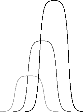
For this is what's really happening. Progress is made in a series of waves. Each starts with a giddy period of exponential growth. That's when it's fun, when everybody's jumping in, working 24 hours a day, losing money hand over fist, and having a wonderful time.
As the curve really begins to soar, it starts having an impact on the established, mature technologies that went before. This is a general-purpose graph; it's my worldview on a single slide. You can read it as transistors replacing vacuum tubes and then being supplanted by integrated circuits, or of mainframes, minicomputers, and personal computers, of turnkey mainframe CAD companies, workstation based CAD, and mass market desktop CAD software, or for that matter of species diversification and extinction in an ecosystem.
It doesn't matter. It's all evolution in action.
Handoff from one technology to the next
| Mechanisms | ⟶ | Electronics |
| Vacuum Tubes | ⟶ | Transistors |
I call the points where a rapidly developing technology takes off and starts to displace its predecessor “technological transitions.” These are perilous times, but they are the times when great industries are founded. Rarely do leaders of the last technology play a significant role in the next; they've usually become encumbered with a bureaucratic superstructure focused on managing a mature market but incapable of acting on the small scale with the rapid pace that's needed to develop its successor—the new market that's inexorably displacing them.
Having grown out of their period of rapid growth, they've forgotten it's possible. They value caution over the very assumption of risk that built their industries in the first place, and through caution, they place at risk everything they have.
Technological transitions are great times to make gobs and gobs of money. Autodesk got on board a relatively minor technological transition in 1982—the second subwave of personal computers, which was a ripple of the microprocessor surge, itself part of the semiconductor tide, contained within the automation industrial revolution. Even so, we managed to turn a hundred thousand dollars into more than a billion in less than eight years.
Just imagine what you could do with a real industrial revolution.
| Tools | 2,000,000 | B.C. |
| Metallurgy | 3600 | B.C. |
| Steam power | 1764 | |
| Mass production | 1908 | |
| Automation | 1946 |
Everybody has their own list of industrial revolutions, and here's mine.
A couple of million years ago we figured out that bashing things with rocks you'd worked into special shapes was better that bonking them with any old random rock you picked up. Suddenly you had tools, craftsmanship, carpentry, weapons, wealth beyond imagining, and global proliferation of a previously obscure critter. This was an information revolution: using knowledge to transform existing materials into useful forms.
All of this was based on natural materials, picked up from the Earth or taken from plants and animals. Then, about 5600 years ago, on a sunny Thursday morning, somebody figured out how to extract copper from yucky looking rocks. Now people had access to new materials—technology was no longer limited by what was lying around; it could make new substances and build with them. This led to bronze, iron, alloys, alchemy, chemistry, and steel. This was a material revolution; enabling new technologies by creating substances not found in nature.
All of industry until the 18th century was powered by the energy of human or animal muscles, or natural energy sources like falling water and the wind. This limited both the scope and scale of what could be done. The advent of practical steam power swept away these limitations, spawning trains, steamboats, satanic mills, and capitalism. This was an energy revolution.
As the scale of industry grew, economies of scale could be realised by standardisation and interchangeability of parts. These trends ultimately led to an entire industrial system focused around mass production of largely identical objects. This is harder to date. I use 1908, the date of the first automobile assembly line, as the milestone of mass production. Mass production was essentially an information revolution: it embodied a uniform set of specifications in huge numbers of objects, thereby reducing their cost so many more people could afford them than ever before.
I consider automation to be the most recent industrial revolution. Until the advent of mechanical, electrical, and electronic computers in the twentieth century, any computation or information processing required the attention of a human being and necessarily proceeded at the pace a human could work. The computer revolution, which I date here from ENIAC in 1946, has been an information revolution that has transformed not only the mechanics of industry, how we make things, but also the structure of our organisations and societies. Ironically, mass production, an essential precursor of automation, is becoming less important as the introduction of intelligence throughout the manufacturing process allows more flexible forms of production.
Before I get into the details of what's about to happen, I want to make sure we understand the territory. We're about to discuss things that range in size by a factor of a billion to one, so it's useful to go over the distance scale so we don't confuse millions and billions the way the politicians do.
Let's start with the measure of all things, a human being. Humans are on the order of metres in size, actually closer to two metres, but we can ignore ones and twos when talking about factors of 1000, as we're about to do.
Most of the history of technology has been built to this scale, and tended to look something like this.
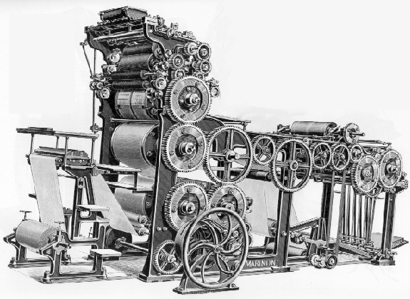
If an object has to be assembled by people, in many cases powered by people, and operated by people, it doesn't make any sense to make it smaller than people can reasonably use, notwithstanding the design of modern car stereos.
The size of mechanical parts is governed by the materials that compose them and the scale of the machines used to fabricate them. Both imposed severe limitations on miniaturisation throughout most of history, limitations that were surmounted only with great difficulty and expense when absolutely necessary, as in the design of watches.
Wherever technology leads us, effective design at this scale will remain important as long as humans use the products. This is the domain of user interface and ergonomics.
If we shrink down by a factor of a thousand, we arrive at the millimetre scale, where an ant is pretty big stuff. This is about the limit of what the human eye can effectively see unaided, or the human body can manipulate without mechanical assistance, so it's a convenient milestone on the road to Lilliput.
Here's an example of millimetre scale technology. This, for those of
you too young to remember or old enough to have had enough bad
experiences and deliberately forgotten, is a vacuum
tube.![]()
If you examine this device closely, you'll see that its fundamental geometry: the spacing of its grid wires, the distance from the cathode to the plate, are all on the order of millimetres. With the development of electronics, device scaling immediately became important: the smaller you made a tube, the faster it ran and the less power it used. Unfortunately, the fact that tubes had to be assembled from separate metal parts limited how much you could shrink them.
This particular tube is a 6SN7. That's the type used in the flip-flop circuit of the ENIAC, the world's first electronic digital computer of 1946. Each tube, along with a handful of other parts, stored one bit of computer memory—RAM. The ENIAC contained 18,000 tubes like this, occupied 3000 cubic feet of space, and required 140 kilowatts of electricity. It had about the computing power of a pocket calculator. It was a miracle of millimetre technology.
Tubes like this aren't even made in the United States any more; this one came from the Soviet Union and cost $13. Interestingly, that's almost exactly the current price of an 80 nanosecond 1 megabit dynamic RAM, with a million times the storage capacity and 125 times the speed.
Which brings us to the next factor of 1000 in size, to the micrometre range that's the heart of microchip technology. All of these RAMs and ROMs and microprocessors have feature sizes on the order of micrometres. The entire march of processor technology I showed in the timing slide is essentially the story of learning to shrink our circuits from the order of tens of micrometres to single micrometres, and the frontier of electronics in the next several years will be shrinking further, down to fractions of a micrometre.
And then what?
Well, that's a very interesting question.

Here's a piece of silicon that's been machined into slabs a third of a micrometre wide. This is about the best we can do right now with conventional processing technology, and to give an indication of just how tiny that is, each of those slabs is smaller than the wavelength of deep violet light.
Needless to say, this image is from an electron microscope, not an optical one.
All the way down to micrometres, we've been able to design circuits essentially the way we did in the days of vacuum tubes. Yes, the devices and fabrication technologies changed, but the rules of the game like Ohm's law remained the same.
Somewhere between half a micrometre and a tenth of a micrometre, these comfortable assumptions begin to break down. The weird world of quantum mechanics, where the wave nature of the electron becomes apparent, begins to become manifest at this scale and straightforward shrinking doesn't seem likely to work.
This suggests we're already uncomfortably near the top of the curve for conventional electronics.
But how far are we from the theoretical bottom?
Just about another factor of a thousand, it turns out.
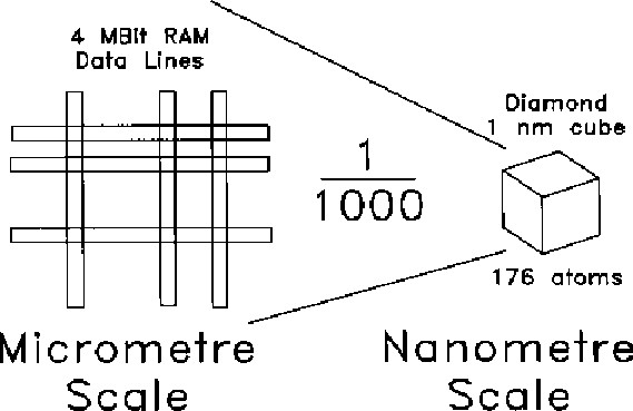
If we shrink from a micrometre to a thousandth of that, a nanometre, we've reached the scale where atoms become tangible objects. A one nanometre cube of diamond has 176 atoms in it.
Designing at this scale is working in a world where physics, chemistry, electrical engineering, and mechanical engineering become unified into an integrated field.
This field will be called molecular engineering, and I believe it will be at the heart of the next two industrial revolutions.
The principles of physics, as far as I can see, do not speak against the possibility of maneuvering things atom by atom. …it is interesting that it would be, in principle, possible (I think) for a physicist to synthesize any chemical substance that the chemist writes down. Give the orders, and the physicist synthesizes it. How? Put the atoms where the chemist says, and so you make the substance.
— Richard Feynman, 1959
Over thirty years ago Richard Feynman pointed out that physicists knew no limits to prevent us from doing engineering at the level of atoms. His words are as true today as the day he spoke them.
Until recently, though, while the lack of physical limits was accepted as commonplace, molecular engineering was thought of as impractical, unnecessary, or requiring breakthroughs in knowledge and technique that placed it somewhere in the distant future.
Many visionaries intimately familiar with the development of silicon technology still forecast it would take between 20 and 50 years before molecular engineering became a reality. This is well beyond the planning horizon of most companies.
But recently, everything has begun to change.
In 1981, Gerd Binnig and Heinrich Rohrer of the IBM Zürich Research Laboratory invented the Scanning Tunneling Microscope. This device, easily one of the most elegant and unanticipated inventions of the century, allowed imaging of individual atoms, and won Binnig and Rohrer the Nobel Prize in Physics for 1986.
In 1985, Binnig and Christoph Gerber of IBM Zürich, along with Calvin Quate of Stanford, invented the atomic force microscope. This allowed imaging nonconductive matter such as living cells to molecular (although not currently atomic) resolution.
Since then, every year has seen new inventions in the rapidly growing field of scanning probe microscopes. They're now imaging bits on magnetic surfaces, measuring temperature at microscopic sites, and monitoring the progress of chemical reactions.
Recently, IBM San Jose used a scanning tunneling microscope to, in Feynman's words, put the atom right where the chemist says.
Here's a picture of xenon atoms on a nickel crystal, lined up in a row by pushing them into place with an STM tip. Remember, those bumps are individual atoms, and they've been moved precisely into position, in a row, one half nanometre from each other.
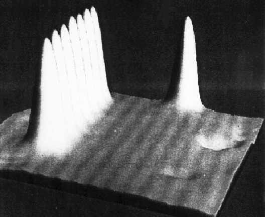
You can not only put atoms right where the chemist wants them, you can put them right where the marketing department says to, as well.
Here, from the same paper, is a sequence of pictures showing a bunch of randomly positioned xenon atoms being aligned to spell out the name of the sponsor.
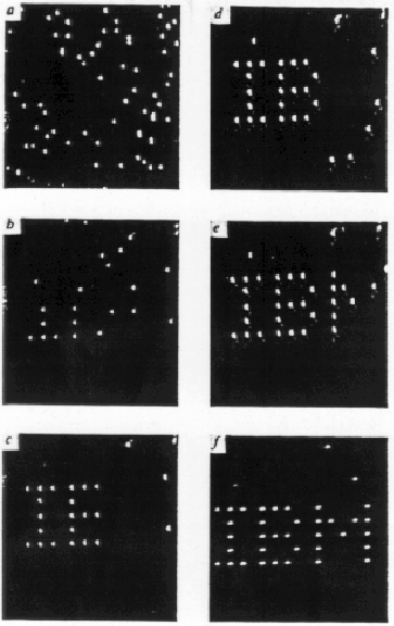
Again, each dot in this picture is a single atom, and the letters are 5 nanometres tall.
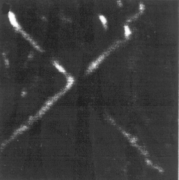
Here's an illustration from a paper published a few weeks before the IBM result. The bottom picture shows an X drawn with an atomic force microscope on material adsorbed onto a zeolite crystal surface. The X is 8 nanometres tall, and it remained intact for the 45 minutes it was monitored after being drawn there.
This experiment was done with a desktop instrument no bigger or more complicated than a compact disc player.
…thorough control of the structure of matter at the molecular level. It entails the ability to build molecular systems with atom-by-atom precision, yielding a variety of nanomachines. These capabilities are sometimes referred to as molecular manufacturing.
— K. Eric Drexler, 1989
A capability never before available to technology. Previously, the exclusive domain of biological systems.
So what we're talking about is making the next big jump to building systems a thousand times smaller than the ones we're making today; to go all the way to the bottom and start working with individual atoms.
This is called molecular engineering, or nanotechnology. Eric Drexler defines this as control of the structure of matter at the molecular level, however achieved.
Technology has never had this kind of precise control; all of our technologies today are bulk technologies. We take a big chunk of stuff and hack away at it until we're left with the object we want, or we assemble parts from components without regard to structure at the molecular level. Precise atomic level fabrication has previously been done only by living biological organisms. We are entering an era when some of the barriers between engineered and living systems will begin to fall.

In fact, we're already building components on the scale of biological systems. The picture on the left shows a neuron net from a human brain with an integrated circuit component inset at the same scale. The picture on the right is a synapse—the interconnection of the wiring in the human brain, with a one micrometre scale. Remember that this is just about the feature size of the wires in our integrated circuits.
The huge difference in capability between engineered and biological systems is not just the materials from which they're made, it's that the fine structure of the integrated circuit stops with what you can see: there's nothing down below. Since we're forced to fabricate our circuits from bulk material, from the top down, they must be essentially two-dimensional. Biology builds its structures from the bottom up, at the molecular level, and in three dimensions.
Engineers are beginning to learn how to do this.
The challenges in scaling another factor of 1000 shouldn't be minimised. Developing millimetre scale electronics and micrometre scale integrated circuits wasn't easy, either, but after we overcame the initial obstacles, both progressed much faster and further than anybody initially expected.
The remarkable thing about molecular engineering is that it looks like there are many different ways to get there and, at the moment, rapid progress is being made along every path—all at the same time.
In 1988, a group at duPont led by William deGrado designed a new protein, called alpha 4 from scratch, and manufactured it in their laboratory. This protein, which never existed in nature, is more stable than natural proteins its size. Researchers around the world are now looking at proteins as molecular structures they can design and build, just as an IC designer lays out a chip.
Chemists are making progress in designing and synthesising molecules that bind to other molecules at specific sites, facilitating the kind of self-assembly that occurs in biology. The 1987 Nobel Prize in chemistry was awarded for just such work.
I've already alluded to the feats accomplished so far with scanning probe microscopes. We now have a tool that lets us see and move individual atoms. STMs have also been used to pin molecules to a substrate and break molecular bonds. John Foster of IBM and Eric Drexler have suggested in a recent paper in Nature that attaching custom molecules to the tip of a scanning microscope may allow assembling objects with up to 10,000 molecular pieces, with atomic precision.
The ability to model and simulate complex molecular systems has been growing rapidly in recent years, driven both by advances in raw computing power, but also by the development of better simulation techniques that now permit modeling of proteins composed of thousands of atoms.
Physicists and electrical engineers are making rapid progress in fabricating electron devices that work at the molecular level. In the past two years, Texas Instruments and Bell Labs have reported molecular-scale quantum transistors and have fabricated quantum wires with X-ray lithography. These quantum wires are on the order of 30 nanometres wide.
Materials scientists and mechanical engineers are fabricating new materials called “nanocomposites,” made up of individual particles ranging from 100 to 1000 atoms. These appear to have electrical and mechanical properties unlike any other engineering materials and may prove useful in the near future.
Even technologies with enormous potential can lie dormant unless there are significant payoffs along the way to reward those that pioneer them. That's one of the reasons integrated circuits developed so rapidly; each advance found an immediate market willing to apply it and enrich the innovator that created it.
Does molecular engineering have this kind of payoff? I think it does.
Remembering that we may be less than 10 years away from hitting the wall as far as scaling our existing electronics, a great deal of research is presently going on in the area of molecular and quantum electronics. The payoff is easy to calculate; you can build devices 1000 times faster, more energy efficient, and cheaper than those we're currently using—at least 100 times better than exotic materials being considered to replace silicon when it reaches its limits.
As an example of current work, consider the molecular optical memory research underway by Prof. Robert Birge and his group at Syracuse University. Using the purple membrane from the bacterium Halobacterium halobium, they've made a working optical bistable switch, fabricated in a monolayer by self-assembly, that reliably stores data with 10,000 molecules per bit. The molecule switches in 500 femtoseconds—that's 1/2000 of a nanosecond, and the actual speed of the memory is currently limited by how fast you can steer a laser beam to the correct spot on the memory.

Lest you think this is some far out distant future research topic, here's an ad from a couple weeks ago by a company in West Germany offering bacteriorhodopsin for sale, listing under applications, “Optical data processing, optical switches, holography, information processing, nonlinear optics, and light sensors.”
And so, we can begin to see the outlines of the sixth industrial revolution: moving from micrometre scale devices to nanometre scale devices. Current progress suggests the revolution may happen within this decade, perhaps starting within five years.
Neither the events nor their consequences will be subtle. Suddenly, we'll acquire new capabilities comparable to those of electronics or computers.
What can we make with it? Well, anything we can design and model that's built of atoms. Think about that. And that includes the essential component of the industrial revolution that will follow, perhaps in the same year.
For once we've mastered the essential technology of life, assembling objects at the molecular level with molecular machines, there's no reason we can't rapidly exploit the central trick of life as well: getting the job done with machines that make copies of themselves.
Mass production has reshaped our industries, lives, economies, and societies, but it's been a limited form of mass production: one where the process of production was explicitly designed and rigidly oriented to making a given object.
Once we can build molecular machines, we can design machines that make copies of themselves. By doing so we achieve the second level of mass production: being able to make anything we can design at a cost fundamentally constrained only by the materials and information it contains.
If this seems absurd, just imagine how an engineer at the start of the twentieth century would have reacted to a description of photolithography, the technology we now use to make integrated circuits and printed circuit boards. “You're telling me you can manufacture objects in the millions just by making photographs of them? Give me a break!”
In fact, if we want to make objects on the metre scale with molecular engineering, we're going to have to design replicating machines. The vacuum tube I showed you has about 1023 atoms in it, and if you try to build something that large atom by atom, it's going to take pretty long. If you add an atom every second, it'll take 1023 seconds which is a real problem because that's a million times longer than the current age of the universe. But, if you can get your molecular machines to crank out copies of themselves, you can set up a chain reaction that can generate numbers on that scale quite rapidly. That's how biology manufactures bacteria, butterflies, and buffaloes, and it works very well.
This is flexible manufacturing taken to the logical limit. An invention made on Monday could, by the following Friday, be in mass production, with billions of copies fabricated. It's the ultimate triumph of information over machinery, of software over hardware, of intellect over capital.
The consequences of this are truly hard to grasp. Just as the development of computers made many problems that have vexed mankind for centuries essentially trivial, we're looking here at the first fundamental change in the means of production in the last two million years. Our economic and societal structures have evolved around assumptions that will no longer be valid once technology reaches this milestone. And it may happen in the next ten years.
But the real question I haven't answered yet is this. “Is it actually possible to make these little tiny machines out of atoms and then get them to replicate themselves, or this all just a pile of hooey, as ridiculous as, say, putting 16 million transistors on a piece of silicon the size of your fingernail?”
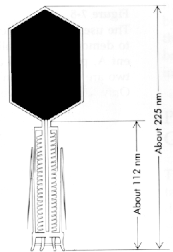
Let's look at how we might design such a machine. Here's a little gadget that looks like a lunar lander, but considerably smaller. It stands about 225 nanometres high. This device is designed to operate within a living system, to seek out cells of a particular type, land on them by extending its landing legs, then inject them with material stored in the tank at the top.
You could design something like this, for example, to locate cancerous cells in a human body and kill them.
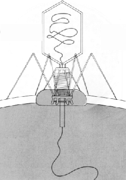
Here's our little machine attached to a cell, with its injector poked through the cell membrane and emptying the tank into the cell's interior.
For a sense of scale, this entire gadget, standing on its tippy-toes would be less than a quarter the size of the smallest feature of a current microprocessor integrated circuit.
Could something like this be built?
Could it possibly work?

Yes. Here's a scanning electron microscope picture of the actual device. It wasn't designed on a CAD system; it evolved in nature. It's called bacteriophage T4. It's a virus that preys on E. coli, a common bacterium that lives in the human intestine.
So molecular devices exist, work, and even succeed in replicating themselves in a proper environment.

Here's an electron micrograph of some E. coli cells infected with another virus, phage f2. The crystalline lattice in the corner of the cell is an array of self-assembled copies of the virus, manufactured within the cell.
You might also ask, “Can we store information at the molecular level?”

The answer to this is also yes, and each of us is living proof.
Here's a picture of a molecular-level file copy operation in progress. This is a 140,000 times blow-up of a strand of messenger RNA being transcribed into the proteins it encodes by a bunch of ribosomes—they're the little beads on the string of RNA. The bumpy strings coming out the sides are the protein chains being assembled by the ribosomes. Each ribosome is a little molecular machine about 20 nanometres across that manufactures proteins to order by reading a tape called messenger RNA and assembling the protein it describes according to the genetic code.
There are quadrillions of them busy at work in each of your bodies at this very moment, and they're about as accurate in copying the molecular data in your DNA as a typical hard disc drive.
Since these biological molecular machines obviously exist, and clearly work, and since biology follows the same laws of physics and chemistry we apply as engineers, there's no question our molecular machines will work. All we have to do is figure out how to design and build them.
And with the rapid progress on all fronts toward molecular fabrication, design may become the most important part of the puzzle.
The consequences of any industrial revolution extend far beyond the domain of scientists and technologists. Indeed, they are difficult to even imagine. For example, try to envision the present world without any electronic devices. You can't. Nobody can. It would be a very different world from ours.
Similarly, the world that will develop after the next two industrial revolutions is difficult to imagine starting from today, but there is every reason to believe the consequences of molecular engineering will be even more profound in every way that those that followed the development of electronics or computers.
One thing, however, is clear. Unlike all of the industrial revolutions that preceded it, molecular engineering requires, as an essential component, the ability to design, model, and simulate molecular structures using computers.
Computer aided design has been largely an adjunct to engineering so far. It has promised productivity gains, cost savings, and other benefits but except at the leading edge, as in VLSI design, has rarely been an indispensable component of the design process.
But with molecules, if you can't model it, you can't build it. Computer aided molecular design is one of the key enabling technologies of these imminent industrial revolutions, and stands to benefit both by helping to bring them about, and to profit from the fruits of their success.
A computer aided design company that comprehends, throughout the organisation, what is about to happen and takes the small, cautious, prudent steps today to position itself to ride this next wave stands an excellent chance of emerging as one of the dominant industries on the planet as molecular engineering supplants our present technological base to the degree that integrated circuits have replaced vacuum tubes and electricity has displaced steam engines.
“Leverage” is commonly used these days in a financial sense to mean
risk/reward amplification through the assumption of debt. But there
are many kinds of leverage. Technological leverage, the power born of
knowledge, is supreme among all forms. We used it to build Autodesk into
the company it is today, fending off competitors with far more money
and people by simply knowing where technology had to go and
hitching a ride.![]()
Autodesk is, at this moment, the preeminent global force in computer aided design. Around the world, technology is poised at the threshold of access to capabilities scarcely imagined a decade ago, and computer aided design is an essential component of this next chapter in the human adventure. The technological leverage of this next industrial revolution is ours, if we want it.
The lever pivots on the micrometre technology of the microprocessor. At one end, we reach to grasp it with our metre scale human hands, at the other, it manipulates atoms to designs born of the human imagination. With this lever, and the knowledge, courage, and vision to operate it wisely, we can truly move the world.
|
|